For the VCO I use a double PLL with two MC145145 since I had still a lot lying around. The schematic of the VCO and PLL, including the micro-controller which handles everything in the transceiver is shown here.
The MC145145 can only handle frequencies up to some 15 MHz, so the frequencies were mixed down. Also, this way I can use two PLL’s with a relatively high reference frequency of 10 kHz to get to a step-size of only 100 Hz! This is how this works:
The main VCO 1 oscillates from 59.3 – 59.8 MHz for 10.7 MHz IF. The VCO 1 signal is mixed with a second VCO 2 to an intermediate frequency of 5-8 MHz which is fed into the first PLL and divided to the reference frequency of this first PLL. The signal from the second VCO 2 signal is on its turn also mixed down to the region 5-8 MHz, this time with a crystal oscillator signal of 48 MHz and than divided to the reference frequency of the second PLL. The two reference frequencies lie 100 Hz apart and were derived from one crystal of in my case 10MHz. I chose fref1 = 10MHz/995 and fref2 = 1005.
In formulas we get:
(fVCO 1 – fVCO 2) = 761 * 10/995
(fVCO2 – fXTAL) = 367 * 10/1005
fXTAL = 48,0000175 MHz.
The 761 and 367 are the divider settings of PLL1 and PLL2 to get to the vco1 frequency of 59.3 MHz (aka the start of the band 70.000 MHz with 10.7 IF). When PLL1 is stepped up and at the same time PLL2 9 is stepped down the result is 100Hz up to 59.300100 MHz. So, using these two PLL’s enables us to have a step size of 100 Hz, while the reference frequency still is rather high at around 10 kHz.
I use a 10 MHz crystal to derive the reference frequencies 10kHz apart but this is not ideal because the step varies up to a few herz depending on the actual frequency. Better would be a 10.1 MHz crystal which is divided by 1010 and 1000 to get 10 and 10.1 kHz reference, but a 10.1 MHz crystal appears hard to get.
In mode FM the step-size is recalculated to 25 kHz. At SSB and CW is it 100 Hz.
RX:
The RF strip at the underside of the chassis, next to the SSB exciter, consists of an RF input and mixer stage, plus an FM detector (mc3357). This part is all build dead bug on a piece of un-etched PCB. The RF preamp and mixer are BF960’s and and in the drain of the mixer FET at 10.7 IF transformer is used, at which secondary coil the signal for the SSB strip is coupled out. The FM crystal filter QMF107 has a high impedance of 2k2 and is coupled directly to the drain of the mixer.
SSB IF:
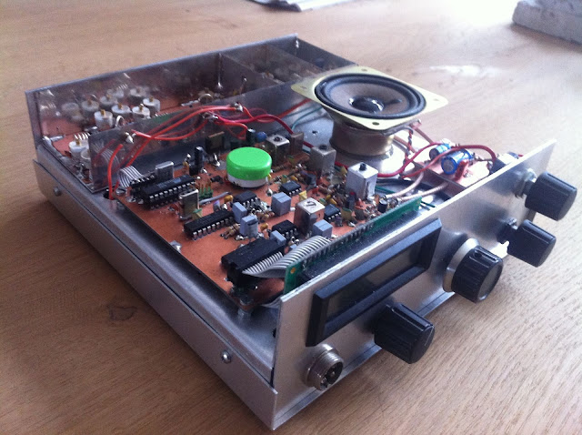
I designed an SSB IF strip including a printed circuit board for this transceiver. Can’t find the schematics at this time but from the component layout this is quite straightforward.
The PCB measures 11 by 11 cm and fits just this way just opposite of the PCB for the VCO/PLL.
TX:
The transmitter consists of a TX mixer (NE612) and a band-pass filter on 70 MHz. In the mixer the VCO signal is mixed with the SSB from the exciter in mode USB/LSB, and with a simple crystal oscillator at 10.7 MHz for FM and CW. In mode FM the main VCO is frequency modulated by the microphone signal. The mic amp is also on the exciter board.
The 70 MHz output is amplified using a BFY90, a BLY87 and a BLW 31 to more than 30W. However, I do have too much amplification in the chain so I need to revise it and eliminate the BLY90 and replace it with for instance a MAV-11. At these relative low frequencies the BLW amplifies more than enough to get up to 20 or 30W. Work in progress here..!
Micro-controller:
The PLL’s but also the display, rotary-encoder and mode switch are all managed by a simple Atmel AVR (AT90S2313 or ATMEGA2313) also on board of the VCO/PLL PCB. This controller can be programmed in circuit via ISP. The software was initially written in assembly, now in C which is much more convenient.


No comments:
Post a Comment